Microcvd is currently developing prototype hardware for a new additive manufacturing process capable of printing durable, heat-resistant metal components on ceramics and other materials. Our prototype systems have been funded by Microcvd and SBIR contracts. The first prototype was successfully demonstrated in early 2019, and a second system capable of performing 3D conformal deposition has been assembled and tested.
We are also developing other additive manufacturing processes and prototype hardware designs, and have received patents for this IP. Microcvd is focused on commercializing these innovations.

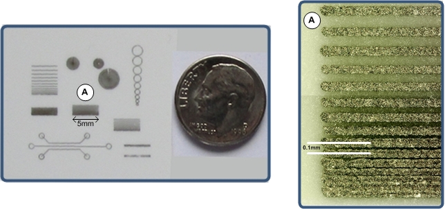
Conductive Nickel patterns on Aluminum Oxide substrate. Right, 2-layer depositions of 100 micron line widths.

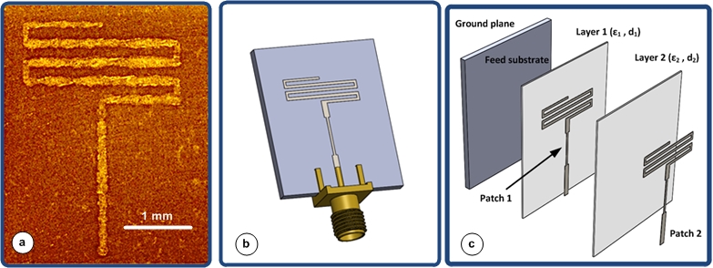
We are printing durable, electrically small parametric antennas (a) Meanderline antenna geometry printed in our prototype, Nickel on magneto-dielectric substrate. Line cross-sectional thickness is adjusted by number of layers; this example is a 2-layer deposit. Antenna line width and thus electrical resistance can be adjusted by changing laser parameters. (b) Notional printed antenna with SMA connector for RF testing. (c) Exploded view of notional stacked antenna assembly featuring multiple layers of dielectrics, antennas, and layer thicknesses. Laser CVD can print conductive patterns and substrates in a single process run.